- 您现在的位置:买卖IC网 > Sheet目录308 > ADZS-BF527-EZLITE (Analog Devices Inc)BOARD EVAL ADSP-BF527
�� �
�
�Blackfin�
�Embedded� Processor�
�ADSP-BF522/ADSP-BF523/ADSP-BF524/ADSP-BF525/ADSP-BF526/ADSP-BF527�
�FEATURES�
�Up� to� 600� MHz� high� performance� Blackfin� processor�
�Two� 16-bit� MACs,� two� 40-bit� ALUs,� four� 8-bit� video� ALUs,�
�40-bit� shifter�
�RISC-like� register� and� instruction� model� for� ease� of�
�programming� and� compiler-friendly� support�
�Advanced� debug,� trace,� and� performance� monitoring�
�Accepts� a� wide� range� of� supply� voltages� for� internal� and� I/O�
��Programmable� on-chip� voltage� regulator� (ADSP-BF523/�
�ADSP-BF525/ADSP-BF527� processors� only)�
�Qualified� for� Automotive� Applications.� See� Automotive�
��289-ball� and� 208-ball� CSP_BGA� packages�
�MEMORY�
�132K� bytes� of� on-chip� memory� (See� Table� 1� on� Page� 3� for� L1�
�and� L3� memory� size� details)�
�External� memory� controller� with� glueless� support� for� SDRAM�
�and� asynchronous� 8-bit� and� 16-bit� memories�
�Flexible� booting� options� from� external� flash,� SPI,� and� TWI�
�memory� or� from� host� devices� including� SPI,� TWI,� and� UART�
�Code� security� with� Lockbox� Secure� Technology�
�one-time-programmable� (OTP)� memory�
�Memory� management� unit� providing� memory� protection�
�WATCHDOG� TIMER�
�PERIPHERALS�
�USB� 2.0� high� speed� on-the-go� (OTG)� with� integrated� PHY�
�IEEE� 802.3-compliant� 10/100� Ethernet� MAC�
�Parallel� peripheral� interface� (PPI),� supporting� ITU-R� 656�
�video� data� formats�
�Host� DMA� port� (HOSTDP)�
�2� dual-channel,� full-duplex� synchronous� serial� ports�
�(SPORTs),� supporting� eight� stereo� I� 2� S� channels�
�12� peripheral� DMAs,� 2� mastered� by� the� Ethernet� MAC�
�2� memory-to-memory� DMAs� with� external� request� lines�
�Event� handler� with� 54� interrupt� inputs�
�Serial� peripheral� interface� (SPI)� compatible� port�
�2� UARTs� with� IrDA� support�
�2-wire� interface� (TWI)� controller�
�Eight� 32-bit� timers/counters� with� PWM� support�
�32-bit� up/down� counter� with� rotary� support�
�Real-time� clock� (RTC)� and� watchdog� timer�
�32-bit� core� timer�
�48� general-purpose� I/Os� (GPIOs),� with� programmable�
�hysteresis�
�NAND� flash� controller� (NFC)�
�Debug/JTAG� interface�
�On-chip� PLL� capable� of� frequency� multiplication�
�OTP� MEMORY�
�RTC�
�VOLTAGE� REGULATOR*�
�JTAG� TEST� AND� EMULATION�
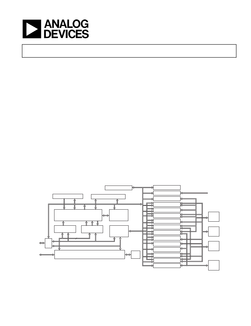
�PERIPHERAL�
�ACCESS� BUS�
�COUNTER�
�SPORT0�
�B�
�INTERRUPT�
�CONTROLLER�
�SPORT1�
�UART1�
�UART0�
�GPIO�
�PORT� F�
�USB�
�L1� INSTRUCTION�
�MEMORY�
�EAB�
�16�
�L1� DATA�
�MEMORY�
�DMA�
�CONTROLLER�
�DCB�
�DEB�
�DMA�
�ACCESS�
�BUS�
�NFC�
�PPI�
�SPI�
�TIMER7-1�
�TIMER0�
�GPIO�
�PORT� G�
�GPIO�
�PORT� H�
�EXTERNAL� PORT�
�FLASH,� SDRAM� CONTROL�
�BOOT�
�ROM�
�EMAC�
�HOST� DMA�
�*REGULATOR� ONLY� AVAILABLE� ON� ADSP-BF523/ADSP-BF525/ADSP-BF527� PROCESSORS�
�Figure� 1.� Processor� Block� Diagram�
�Blackfin� and� the� Blackfin� logo� are� registered� trademarks� of� Analog� Devices,� Inc.�
�Rev.� D�
��Information� furnished� by� Analog� Devices� is� believed� to� be� accurate� and� reliable.�
�However,� no� responsibility� is� assumed� by� Analog� Devices� for� its� use,� nor� for� any�
�TWI�
�PORT� J�
�infringements� of� patents� or� other� rights� of� third� parties� that� may� result� from� its� use.�
�Specifications� subject� to� change� without� notice.� No� license� is� granted� by� implication�
�or� otherwise� under� any� patent� or� patent� rights� of� Analog� Devices.� Trademarks� and�
�registered� trademarks� are� the� property� of� their� respective� owners.�
�One� Technology� Way,� P.O.� Box� 9106,� Norwood,� MA� 02062-9106� U.S.A.�
�Tel:� 781.329.4700� ?2013� Analog� Devices,� Inc.� All� rights� reserved.�
��发布紧急采购,3分钟左右您将得到回复。
相关PDF资料
ADZS-BF533-EZLITE
KIT W/BOARD EVAL FOR ADSP-BF533
ADZS-BF538F-EZLITE
BOARD EVAL FOR ADSP-BF538
ADZS-BF561-EZLITE
BOARD EVAL ADSP-BF561
ADZS-BF592-EZLITE
KIT EVAL EZ LITE ADZS-BF592
ADZS-BF609-EZBRD
KIT EVAL EZ-BOARD ADSP-BF60X
ADZS-HPUSB-ICE
TOOL EMULATOR USB HP CROSSCORE
ADZS-ICE-100B
EMULATOR BLACKFIN
AK-Y1301
CABLE SCSI-3 EXTENSION 68CONDUCT
相关代理商/技术参数
ADZS-BF527-EZLITE
制造商:Analog Devices 功能描述:ADSP-BF527 EZ-KIT Lite Evaluation Kit
ADZS-BF527-MPSKIT
功能描述:BOARD EVAL MEDIA PLAYER BF527 RoHS:是 类别:编程器,开发系统 >> 通用嵌入式开发板和套件(MCU、DSP、FPGA、CPLD等) 系列:- 标准包装:1 系列:PICDEM™ 类型:MCU 适用于相关产品:PIC10F206,PIC16F690,PIC16F819 所含物品:板,线缆,元件,CD,PICkit 编程器 产品目录页面:659 (CN2011-ZH PDF)
ADZS-BF533-EZLITE
功能描述:KIT W/BOARD EVAL FOR ADSP-BF533 RoHS:是 类别:编程器,开发系统 >> 通用嵌入式开发板和套件(MCU、DSP、FPGA、CPLD等) 系列:Blackfin® 产品培训模块:Blackfin® Processor Core Architecture Overview
Blackfin® Device Drivers
Blackfin® Optimizations for Performance and Power Consumption
Blackfin® System Services 特色产品:Blackfin? BF50x Series Processors 标准包装:1 系列:Blackfin® 类型:DSP 适用于相关产品:ADSP-BF548 所含物品:板,软件,4x4 键盘,光学拨轮,QVGA 触摸屏 LCD 和 40G 硬盘 配用:ADZS-BFBLUET-EZEXT-ND - EZ-EXTENDER DAUGHTERBOARDADZS-BFLLCD-EZEXT-ND - BOARD EXT LANDSCAP LCD INTERFACE 相关产品:ADSP-BF542BBCZ-4A-ND - IC DSP 16BIT 400MHZ 400CSBGAADSP-BF544MBBCZ-5M-ND - IC DSP 16BIT 533MHZ MDDR 400CBGAADSP-BF542MBBCZ-5M-ND - IC DSP 16BIT 533MHZ MDDR 400CBGAADSP-BF542KBCZ-6A-ND - IC DSP 16BIT 600MHZ 400CSBGAADSP-BF547MBBCZ-5M-ND - IC DSP 16BIT 533MHZ MDDR 400CBGAADSP-BF548BBCZ-5A-ND - IC DSP 16BIT 533MHZ 400CSBGAADSP-BF547BBCZ-5A-ND - IC DSP 16BIT 533MHZ 400CSBGAADSP-BF544BBCZ-5A-ND - IC DSP 16BIT 533MHZ 400CSBGAADSP-BF542BBCZ-5A-ND - IC DSP 16BIT 533MHZ 400CSBGA
ADZS-BF533-EZLITE
制造商:Analog Devices 功能描述:Microcontroller Development Tool
ADZS-BF533-MMSKIT
功能描述:KIT STARTER MULTIMEDIA BF533 RoHS:是 类别:编程器,开发系统 >> 通用嵌入式开发板和套件(MCU、DSP、FPGA、CPLD等) 系列:Blackfin® 标准包装:1 系列:PICDEM™ 类型:MCU 适用于相关产品:PIC10F206,PIC16F690,PIC16F819 所含物品:板,线缆,元件,CD,PICkit 编程器 产品目录页面:659 (CN2011-ZH PDF)
ADZS-BF537-ASKIT
功能描述:BOARD EVAL SKIT ADSP-BF537 RoHS:是 类别:编程器,开发系统 >> 通用嵌入式开发板和套件(MCU、DSP、FPGA、CPLD等) 系列:Blackfin® 产品培训模块:Blackfin® Processor Core Architecture Overview
Blackfin® Device Drivers
Blackfin® Optimizations for Performance and Power Consumption
Blackfin® System Services 特色产品:Blackfin? BF50x Series Processors 标准包装:1 系列:Blackfin® 类型:DSP 适用于相关产品:ADSP-BF548 所含物品:板,软件,4x4 键盘,光学拨轮,QVGA 触摸屏 LCD 和 40G 硬盘 配用:ADZS-BFBLUET-EZEXT-ND - EZ-EXTENDER DAUGHTERBOARDADZS-BFLLCD-EZEXT-ND - BOARD EXT LANDSCAP LCD INTERFACE 相关产品:ADSP-BF542BBCZ-4A-ND - IC DSP 16BIT 400MHZ 400CSBGAADSP-BF544MBBCZ-5M-ND - IC DSP 16BIT 533MHZ MDDR 400CBGAADSP-BF542MBBCZ-5M-ND - IC DSP 16BIT 533MHZ MDDR 400CBGAADSP-BF542KBCZ-6A-ND - IC DSP 16BIT 600MHZ 400CSBGAADSP-BF547MBBCZ-5M-ND - IC DSP 16BIT 533MHZ MDDR 400CBGAADSP-BF548BBCZ-5A-ND - IC DSP 16BIT 533MHZ 400CSBGAADSP-BF547BBCZ-5A-ND - IC DSP 16BIT 533MHZ 400CSBGAADSP-BF544BBCZ-5A-ND - IC DSP 16BIT 533MHZ 400CSBGAADSP-BF542BBCZ-5A-ND - IC DSP 16BIT 533MHZ 400CSBGA
ADZS-BF537-EZLITE
功能描述:BOARD EVAL ADSP-BF537 RoHS:是 类别:编程器,开发系统 >> 通用嵌入式开发板和套件(MCU、DSP、FPGA、CPLD等) 系列:Blackfin® 产品培训模块:Blackfin® Processor Core Architecture Overview
Blackfin® Device Drivers
Blackfin® Optimizations for Performance and Power Consumption
Blackfin® System Services 特色产品:Blackfin? BF50x Series Processors 标准包装:1 系列:Blackfin® 类型:DSP 适用于相关产品:ADSP-BF548 所含物品:板,软件,4x4 键盘,光学拨轮,QVGA 触摸屏 LCD 和 40G 硬盘 配用:ADZS-BFBLUET-EZEXT-ND - EZ-EXTENDER DAUGHTERBOARDADZS-BFLLCD-EZEXT-ND - BOARD EXT LANDSCAP LCD INTERFACE 相关产品:ADSP-BF542BBCZ-4A-ND - IC DSP 16BIT 400MHZ 400CSBGAADSP-BF544MBBCZ-5M-ND - IC DSP 16BIT 533MHZ MDDR 400CBGAADSP-BF542MBBCZ-5M-ND - IC DSP 16BIT 533MHZ MDDR 400CBGAADSP-BF542KBCZ-6A-ND - IC DSP 16BIT 600MHZ 400CSBGAADSP-BF547MBBCZ-5M-ND - IC DSP 16BIT 533MHZ MDDR 400CBGAADSP-BF548BBCZ-5A-ND - IC DSP 16BIT 533MHZ 400CSBGAADSP-BF547BBCZ-5A-ND - IC DSP 16BIT 533MHZ 400CSBGAADSP-BF544BBCZ-5A-ND - IC DSP 16BIT 533MHZ 400CSBGAADSP-BF542BBCZ-5A-ND - IC DSP 16BIT 533MHZ 400CSBGA
ADZS-BF537-STAMP
功能描述:SYSTEM DEV FOR ADSP-BF537 RoHS:是 类别:编程器,开发系统 >> 通用嵌入式开发板和套件(MCU、DSP、FPGA、CPLD等) 系列:Blackfin® 产品培训模块:Blackfin® Processor Core Architecture Overview
Blackfin® Device Drivers
Blackfin® Optimizations for Performance and Power Consumption
Blackfin® System Services 特色产品:Blackfin? BF50x Series Processors 标准包装:1 系列:Blackfin® 类型:DSP 适用于相关产品:ADSP-BF548 所含物品:板,软件,4x4 键盘,光学拨轮,QVGA 触摸屏 LCD 和 40G 硬盘 配用:ADZS-BFBLUET-EZEXT-ND - EZ-EXTENDER DAUGHTERBOARDADZS-BFLLCD-EZEXT-ND - BOARD EXT LANDSCAP LCD INTERFACE 相关产品:ADSP-BF542BBCZ-4A-ND - IC DSP 16BIT 400MHZ 400CSBGAADSP-BF544MBBCZ-5M-ND - IC DSP 16BIT 533MHZ MDDR 400CBGAADSP-BF542MBBCZ-5M-ND - IC DSP 16BIT 533MHZ MDDR 400CBGAADSP-BF542KBCZ-6A-ND - IC DSP 16BIT 600MHZ 400CSBGAADSP-BF547MBBCZ-5M-ND - IC DSP 16BIT 533MHZ MDDR 400CBGAADSP-BF548BBCZ-5A-ND - IC DSP 16BIT 533MHZ 400CSBGAADSP-BF547BBCZ-5A-ND - IC DSP 16BIT 533MHZ 400CSBGAADSP-BF544BBCZ-5A-ND - IC DSP 16BIT 533MHZ 400CSBGAADSP-BF542BBCZ-5A-ND - IC DSP 16BIT 533MHZ 400CSBGA